User Tools

Site Tools


project:weathersonde:pcb

PCB and schematic

Reverseingeneering Vaisala weather sonde PCB, creating schematics.

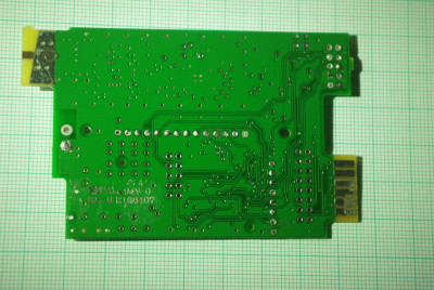
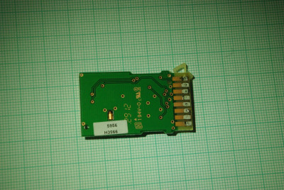
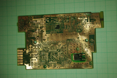
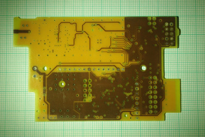
The following pictures capture all 4 PCB copper layers and component placement.

TODO:

  • try fix photo deformation and missalignment in order to create precise overlap.
  • draw schematics
  • find out values of components
  • main PCB back side top layer
    main PCB back side top layer
  • main PCB front side top layer
    main PCB front side top layer
  • sensors PCB front side
    sensors PCB front side
  • sensors PCB back side
    sensors PCB back side
  • main PCB front side top layer - with removed curcuits
    main PCB front side top layer - with removed curcuits
  • main PCB xxx side bottom layer
    main PCB xxx side bottom layer
project/weathersonde/pcb.txt · Last modified: 2018/09/24 11:25 by pinky