PCB and schematic
Reverseingeneering Vaisala weather sonde PCB, creating schematics.
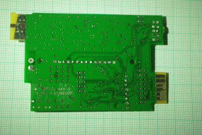
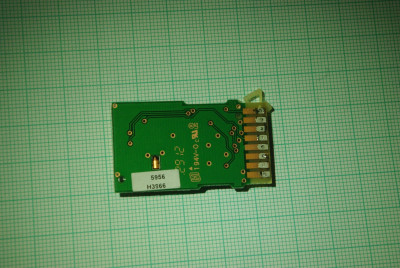
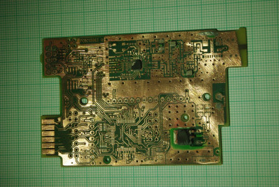
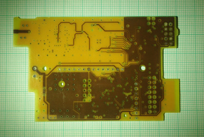
The following pictures capture all 4 PCB copper layers and component placement.
TODO:
- try fix photo deformation and missalignment in order to create precise overlap.
- draw schematics
- find out values of components


